
The ability to monitor biological environments in real time with wireless devices is a powerful tool for a wide variety of implementations, from implanted insulin pumps for diabetics to biosensors for bacteriological infections.[1] While these devices are being developed, one of the major hurdles that the implementation is facing is a power source. The bulkiness of batteries makes them an impractical choice, especially since the chemistry of such small batteries would need to be highly efficient and the materials required to do so are rarely biologically safe. Therefore, the development of a material that generates electricity on a scale appropriate for wireless nanotech is essential and the subject of Zhong Lin Wang and Jinhui Song’s latest discovery. They aim to utilize some of the movement that naturally occurs in a biological environment as a power source. This is achieved through the combination of piezoelectronics, a property that is present in select materials and is characterized by a buildup of electric charge in response to applied mechanical stress, with semiconductor properties. The compound that has both of these properties and is biologically safe is Zinc Oxide (ZnO).
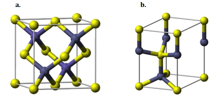
Figure 1. The zinc-blende (a) and wurtzite type (b) structures.
While ZnO has been consistently used by mankind since the smelting of brass and its semiconductor properties have been under investigation since the 1930s, new uses for the compound are still being discovered.2 ZnO is distinct from many of the other semiconductors from the II-VI group, named for the groups from the periodic table that the individual compounds are found, because of the large difference in electronegativity between the two atoms. The bond between oxygen, a highly electronegative element, and zinc, an atom with very low electronegativity, has such uneven electron distribution between the two atoms that the individual elements can essentially be treated as ions.[2] This results in a unique crystal structure when compared to the other group II-VI semiconductors. The bonds in ZnO are oriented in a tetrahedral geometry, and the two crystal structures associated with this geometry are zinc-blende and wurtzite (Figure 1). While other group II-VI semiconductors tend to organize themselves in the zinc-blende structure, the polarity in the ZnO bonds predisposes the compound into crystalizing in primarily the wurtzite type structure though the chemistry behind this predisposition is still unclear. The wurtzite type structure lacks of inversion symmetry – there is no space in where the atoms can be reflected through one point and have the resulting structure be identical to the one before the symmetry operation- which results in compounds with this structure behaving piezoelectrically. This happens because when stress is applied at the apex of the tetrahedrally coordinated Zn+2 and O2- ions the centers of the cations and anions are displaced, inducing a dipole moment. This is repeated along all the cells in a crystal and causes a macroscopic potential (piezopotential) drop along the strain direction.[3]
With these properties of ZnO in mind, Zhong Lin Wang and Jinhui Song successfully grew nanowires on a thin gold plate, and ran the conductive tip of an atomic force microscope (AFM) across the structure to release around 0.6 pW assuming the nanowire resonance frequency of around 10 MHz. This happens because as the tip asserts a horizontal force against one side of the nanowire it causes it to bend away, resulting in a stretching of the molecules on the side of the nanowire in contact with the AFM tip and a compression of the ones on the other side. Because of ZnO’s piezoelectric properties, this induces a charge separation across the nanowire. While 0.6 pW is a very small amount of energy, it scales up to around 10 pW/μm2 when the density of nanowires is taken into consideration. Because the power requirements of nanotech are relatively small, they could successfully be powered with a ZnO nanowire array that is 10 μm x 10 μm.[3] While there is still much room for improvement in the efficiency of 17-30%, it is an exciting combination of piezoelectric and semiconductor properties made possible through the unique structure of ZnO. By taking the first steps in creating a nanogenerator that creates electricity from physical stress, nanotechnology that can remotely monitor biological environments to regulate insulin levels or detect bacterial infections is no longer as severely limited by its power source.
Scientific References:
1. Malsch Industrial Physicist 2002, 8.3, 15-17.
2. Klingshirn, Chem. ChemPhysChem 2007, 8.6, 782-803.
3. Wang and Song Science 2006, 312, 242-245
Media References:
Zinc blende structure: http://commons.wikimedia.org/wiki/File:Sphalerite-unit-cell-3D-balls.png
Wurtzite structure: http://commons.wikimedia.org/wiki/File:Wurtzite-unit-cell-3D-balls.png